作为 ARM 嵌入式 工程师, 下载调试器都应该知道,但你真正了解SWD如何下载调试的么?ARM 芯片通过什么物理 接口和什么方式连接完全取决于芯片Debug子系统的架构如何?
你可以从芯片手册的Debug章节获得DAP(Debug Access Port)的 信息。我调试的是 NXP 公司 最新车载芯片S32K3系列的芯片,从S32K3xx Reference Manual中Debug 子系统章节中得知该芯片的debug和Trace接口基于Arm CoreSight SoC-400的标准。 从Arm CoreSight SoC-400 Techn ical Reference Manual章节Debug Access Port中你可以获取到详细的信息。这里只做关键内容介绍,只介绍涉及的部分。
参考文档:Arm CoreSight SoC-400 Technical Reference Manual , CoreSight Components Technical Reference Manual , Arm CoreSight Architecture Specification。
从Arm CoreSight SoC-400 Technical Reference Manual中Figure 4-1 Structure of the CoreSight SoC-400 DAP components看出SWD只是接入芯片调试子系统的一种方式而已。
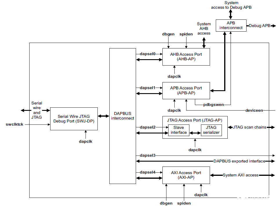
那么外部调试工具是怎么通过SWD的方式接入到ARM核内部的呢?下面我们详细介绍一下CoreSight SoC-400 DAP组件架构。
DAP是片外调试工具接入SOC组件的集合。访问方式是按照ARM®调试接口架构规范 ADIv5.0~ ADIv5.2实现。
DAP由以下组件组成:
•DP用于管理与外部调试器的连接。
•AP访问片上系统资源。 每种类型的AP可以有多个。
•DAPBUS互连,用于将DP连接到一个或多个AP。
AP提供了非侵入式访问权限:
•CoreSight组件下载或者烧录模型。 通常是通过系统级CoreSight APB总线和APB-AP来完成的。
•内存映射的系统组件,通常使用AXI-AP或AHB-AP。
•使用JTAG-AP的旧版JTAG配置的调试组件。
而且,某些支持CoreSight的 处理器直接连接到DAPBUS互连,并实现自己的ADIv5兼容AP。
CoreSight SoC具有单个多功能DP,如下所示:
SWJ-DP 这是一个组合调试 端口,可以通过ADIv5.1定义的JTAG或串行线协议进行 通信。它包含两个调试端口SW-DP和JTAG-DP,您可以通过接口时序命令选择它们,以在调试端口接口之间切换。
JTAG-DP 兼容DP架构版本0。SW-DP兼容DP架构版本2和Serial Wire协议版本2,使SW-DP可以与其他SW-DP或其他实现组件共享连接。
CoreSight SoC中包含的AP端口是:
AXI-AP AXI-AP实现了ADIv5存储器访问端口(MEM-AP)架构,以直接连接到AXI存储器系统。 您可以使用适当的桥接组件将其连接到其他内存系统。
AHB-AP AHB-AP提供了一个AHB-Lite主站,用于访问系统AHB总线。 这兼容ADIv5.1中的MEM-AP并且可以执行8到32位访问。
APB-AP APB-AP在AMBA v3.0中提供了一个APB主设备,用于访问调试APB总线。 这兼容具有32位固定传输大小的MEM-AP体系结构。
JTAG-AP JTAG-AP提供对片上组件的JTAG访问,用作JTAG主端口以驱动 ASIC中的JTAG链。 这是ADIv5.1中JTAG-AP的实现。
DAPBUS 互连将DP连接到AP。 系统可能不包含某些类型的AP,或者可能包含多个相同类型的AP。
单纯看CoreSight SoC-400 DAP组件架构,感觉会比较空洞,我们结合一下S32K3XX DAP架构图来看一下。
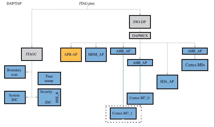
从芯片的DAP architecture,不难看出S32K3采用的是Arm®CoreSight™架构。
你基本可以找到 CoreSight SoC-400和S32K3XX的DAP architecture对应关系:
S32K3XX CoreSight SoC-400
SWJ-DAP <--> Serial Wire JTAG Debug Port (SWJ-DP)
DAPMUX <--> DAPBUS interconnect
AHB_AP <--> AHB Access Port (AHB-AP)
APB-AP <--> APB Access Port (APB-AP)
MDM_AP <--> DAPBUS exported interface
SDA_AP <--> DAPBUS exported interface
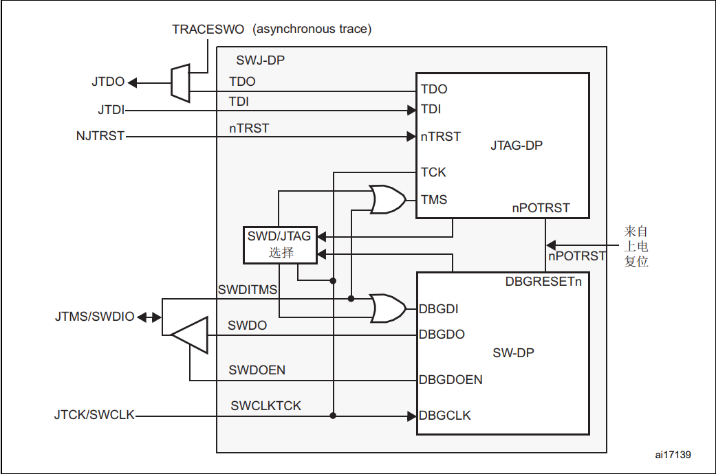
SWJ-DP由JTAG-DP和SW-DP的组成。 它选择JTAG或SWD作为连接机制,并启用JTAG-DP或SW-DP作为DAP的接口。
JTAG和SWD接口
JTAG接口具有四个强制引脚tck,tms,tdi和tdo,以及一个可选的复位引脚ntrst。 JTAG-DP和SW-DP还需要独立的上电复位npotrst。
SWD接口需要两个引脚:
•双向swdio 信号。
• 时钟swclk,可以从设备输入或输出。
为了使JTAG或SWD共享 连接器,必须在SWJ-DP模块外部进行连接。 特别是,tms必须是双向引脚,以支持SWD模式下的双向swdio引脚。
20- Pin ARM Standard JTAG Connector
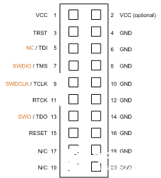
(From https://www2. keil.com/coresight/coresight-connectors)
它支持用于访问基于ARM7和ARM9的设备的JTAG接口。 对于Cortex-Mx设备,它支持串行线和JTAG接口,以访问Cortex-Mx设备上可用的所有SWD,SWV和JTAG信号。
那么是调试工具是通过什么方式访问Cortex-Mx内部的呢?
参考文档:ARM® Debug Interface Architecture Specification ADIv5.0 to ADIv5.2
DAP访问方式是按照ARM®调试接口架构规范ADIv5.0~ADIv5.2实现。
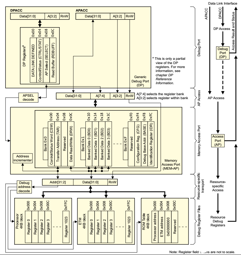
DAP****结构框图如下:
来自ARM® Debug Interface Architecture Specification ADIv5.0 to ADIv5.2的Figure A1-2 Structure of the DAP, showing DPv0 JTAG-DP accesses to a generic AP
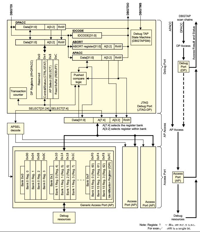
ADI包括:
Debug Access Port (DAP),DAP外部物理连接 和 DAP与内部调试资源组件的连接。
DAP包含两个逻辑模块,Debug Port(DP) 和 Access Port(AP)。DP来连接外部的host,AP来访问内部的调试组件 寄存器:
• Access to the Debug Port (DP) registe rs. This is provided by Debug Port accesses (DPACC).
• Access to the Access Port (AP) registers. This is provided by Access Port accesses (APACC)
ADIv5标准外部接口支持一下几种DP:
• The JTAG Debug Port (JTAG-DP)
• The Serial Wire Debug Port (SW-DP)
• The Serial Wire/JTAG Debug Port (SWJ-DP)
内部资源接口包含:
AP (MEM-AP or JTAG-AP)
由于我选择使用的是SW-DP的方式访问,我这里只对SWD协议处理流程介绍。
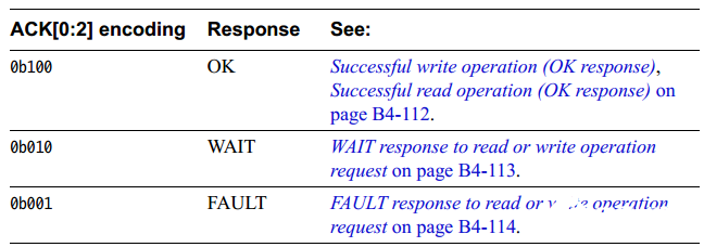
我们下面剖析一下SW-DP报文格式(担心翻译有误,就用英文原文):
Start A single start bit, with value 0b1.
APnDP A single bit, indica ting whether the Debug Port or the Access Port Access register is to be accessed. This bit is 0b0 for a DPACC access, or 0b1 for an APACC access.
RnW A single bit, indicating whether the access is a read or a write. This bit is 0b0 for a write access, or 0b1 for a read access.
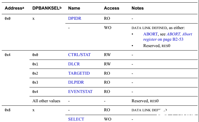
A[2:3] Two bits, giving the A[3:2] address field for the DP or AP register Address:
• For a DPACC access, the register being addressed depends on the A[3:2] value and, if A[3:2]==0b01, the value that is held in SELECT. DPBANKSEL. For det ails, see:
— DP architecture version 1 (DPv1) address map on page B2-50
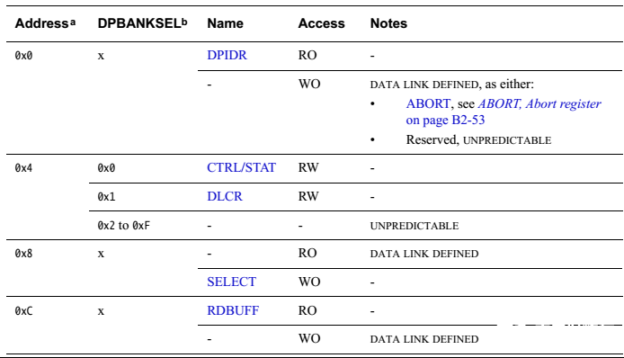
— DP architecture version 2 (DPv2) address map on page B2-51.
• For an APACC access, the register being addressed depends on the A[3:2] value and the value
that is held in SELECT.{APSEL,APBANKSEL}. For details about addressing, see:
— MEM-AP Prog rammers’ Model on page C2-169 for accesses to a MEM-AP register
— JTAG-AP register summary on page C3-206 for accesses to a JTAG-AP register.
Note
The A[3:2] value is transmitted Least Significant Bit (LSB) first on the wire, which is why it appears as A[2:3] on the diagrams.
Parity A single parity bit for the preceding packet. See Parity on page B4-108.
Stop A single stop bit. In the synchronous SWD protocol, this bit is always 0b0.
Park A single bit. The host must drive the Park bit HIGH to park the line before tristating it for the turnaround period, to ensure that the line is read as HIGH by the target, which is required because the pull-up on the SWD interface is weak. The target reads this bit as 0b1.
Trn Turnaround. See Line turnaround on page B4-107.
Note
All the examples that are given in this chapter show the default turnaround period of one cycle.
ACK[0:2] A three-bit target-to-host response.
WDATA[0:31]
32 bits of write data, from host to target.
RDATA[0:31]
32 bits of read data, from target to host
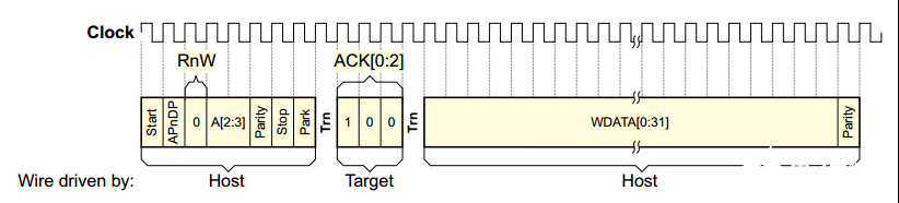
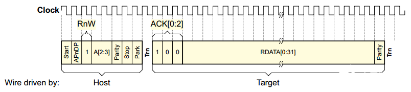
我们已经了解了报文格式,那我们结合SWD的报文读写时序图来理解。
Successful write operation (OK response)
Successful read operation (OK response)
下面我结合Successful write operation (OK response)和Structure of the Debug Access Port举个例子演示一下SWD如何控制DAP。
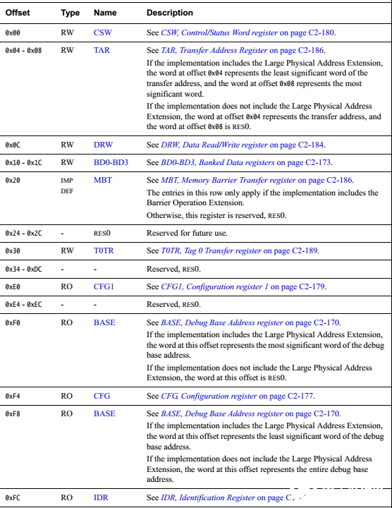
Every AP or DP access transaction from the debugger includes two address bits, A[3:2]:
• For a DP register access, the address bits A[3:2] and SELECT.DPBANKSEL determine which register is accessed. SELECT is a DP register.
• For an AP register access, SELECT.APSEL selects an AP to access, and the address bits A[3:2] are combined with SELECT.APBANKSEL to determine which AP register is accessed, as summarized in Structure of the Debug Access Port. That is, the two address bits A[3:2] are decoded to select one of the four 32-bit words from the register bank indicated by SELECT.APBANKSEL in the AP indicated by SELECT.APSEL. Bits [1:0] of all AP and DP register addresses are 0b00.
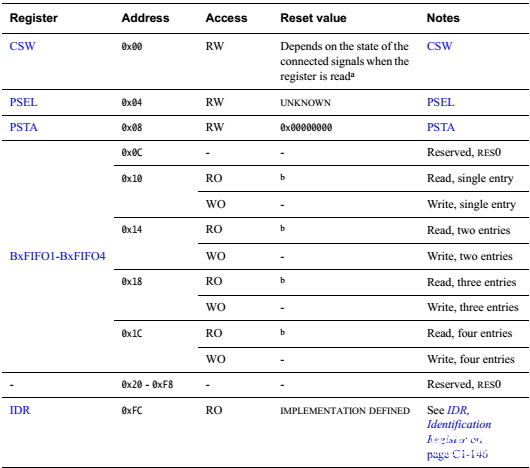
假如我要向AP0寄存器0x14里写入0xF0000001,调试工具操作流程如下:
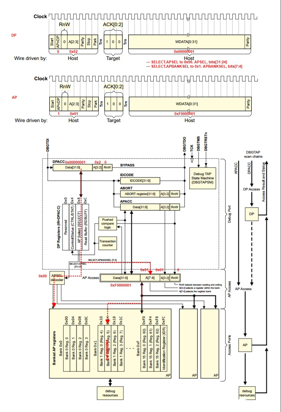
使用DP寄存器向DP的SELECT寄存器写入:
— SELECT.APSEL to 0x00. APSEL, bits[31:24]
— SELECT.APBANKSEL to 0x1. APBANKSEL, bits[7:4]
APnDP 写0 表示DP操作,A[3:2]写0x02表示操作0x08 SELECT 寄存器。写入0x00000001.
使用AP寄存器向AP0的0x14寄存器写入:
APnDP 写1 表示AP操作,由于已经向DP的SELECT选择了APBANKSEL为0x01,A[3:2]写0x01表示操作0x14 寄存器。写入0xF0000001. 在这个情况下能访问0x10~0x1C等4个寄存器。
其他AP操作其实流程一样。
下面我稍微了解一下MEM-AP.
来自 ARM® Debug Interface Architecture Specification ADIv5.0 to ADIv5.2的Figure C2-1 MEM-AP connecting the DP to debug components
说白了MEM-AP为DAP提供了一种直接访问系统地址空间的访问。操作其实和通用AP的访问一样。MEM-AP访问系统地址空间,其实有多了一层间接访问。我们直接从OpenOCD源码中看整个过程。
https://sourceforge.net/p/openocd/code/ci/v0.11.0/tree/src/target/cortex_m. c#l2521
struct target_type cortexm_target = {
.name = "cortex_m",
.deprecated_name = "cortex_m3",
.poll = cortex_m_poll,
.arch_state = armv7m_arch_state,
.target_request_data = cortex_m_target_request_data,
.halt = cortex_m_halt,
.resume = cortex_m_resume,
.step = cortex_m_step,
.assert_reset = cortex_m_assert_reset,
.deassert_reset = cortex_m_deassert_reset,
.soft_reset_halt = cortex_m_soft_reset_halt,
.get_gdb_arch = arm_get_gdb_arch,
.get_gdb_reg_list = armv7m_get_gdb_reg_list,
.read_memory = cortex_m_read_memory,
.write_memory = cortex_m_write_memory,
.checksum_memory = armv7m_checksum_memory,
.blank_check_memory = armv7m_blank_check_memory,
.run_algorithm = armv7m_run_algorithm,
.start_algorithm = armv7m_start_algorithm,
.wait_algorithm = armv7m_wait_algorithm,
.add_breakpoint = cortex_m_add_breakpoint,
.remove_breakpoint = cortex_m_remove_breakpoint,
.add_watchpoint = cortex_m_add_watchpoint,
.remove_watchpoint = cortex_m_remove_watchpoint,
.commands = cortex_m_command_handlers,
.target_create = cortex_m_target_create,
.target_jim_configure = adiv5_jim_configure,
.init_target = cortex_m_init_target,
.examine = cortex_m_examine,
.deinit_target = cortex_m_deinit_target,
.profiling = cortex_m_profiling,
};
OpenOCD通过DAP MEM AP的访问实现Cortex M系统地址空间的访问。
cortex_m_read_memory和cortex_m_write_memory实现了读写操作。看一下这两个函数是怎么实现的。
cortex_m_read_memory实现
static int cortex_m_read_memory(struct target *target, target_addr_t address,
uint32_t size, uint32_t count, uint8_t *buffer)
{
struct armv7m_common *armv7m = target_to_armv7m(target);
if (armv7m->arm.is_armv6m) {
/* armv6m does not handle unaligned memory access */
if (((size == 4) && (address & 0x3u)) || ((size == 2) && (address & 0x1u)))
return ERROR_TARGET_UNALIGNED_ACCESS;
}
return mem_ap_read_buf(armv7m->debug_ap, buffer, size, count, address);
}
int mem_ap_read_buf(struct adiv5_ap *ap,
uint8_t *buffer, uint32_t size, uint32_t count, uint32_t address)
{
return mem_ap_read(ap, buffer, size, count, address, true);
}
/**
* Synchronous read of a block of memory, using a specific access size.
*
* @param ap The MEM-AP to access.
* @param buffer The data buffer to receive the data. No particular alignment is assumed.
* @param size Which access size to use, in bytes. 1, 2 or 4.
* @param count The number of reads to do (in size units, not bytes).
* @param adr Address to be read; it must be readable by the currently selected MEM-AP.
* @param addrinc Whether the target address should be increased after each read or not. This
* should normally be true, except when reading from e.g. a FIFO.
* @return ERROR_OK on success, otherwise an error code.
*/
static int mem_ap_read(struct adiv5_ap *ap, uint8_t *buffer, uint32_t size, uint32_t count,
uint32_t adr, bool addrinc)
{
struct adiv5_dap *dap = ap->dap;
size_t nbytes = size * count;
const uint32_t csw_addrincr = addrinc ? CSW_ADDRINC_SINGLE : CSW_ADDRINC_OFF;
uint32_t csw_size;
uint32_t address = adr;
int retval = ERROR_OK;
/* TI BE-32 Quirks mode:
* Reads on big-endian TMS570 behave strangely differently than writes.
* They read from the physical address requested, but with DRW byte-reversed.
* For example, a byte read from address 0 will place the result in the high bytes of DRW.
* Also, packed 8-bit and 16-bit transfers seem to sometimes return garbage in some bytes,
* so avoid them. */
if (size == 4)
csw_size = CSW_32BIT;
else if (size == 2)
csw_size = CSW_16BIT;
else if (size == 1)
csw_size = CSW_8BIT;
else
return ERROR_TARGET_UNALIGNED_ACCESS;
if (ap->unaligned_access_bad && (adr % size != 0))
return ERROR_TARGET_UNALIGNED_ACCESS;
/* Allocate buffer to hold the sequence of DRW reads that will be made. This is a significant
* over-allocation if packed transfers are going to be used, but determining the real need at
* this point would be messy. */
uint32_t *read_buf = calloc(count, sizeof(uint32_t));
/* Multiplication count * sizeof(uint32_t) may overflow, calloc() is safe */
uint32_t *read_ptr = read_buf;
if (read_buf == NULL) {
LOG_ERROR("Fai led to allocate read buffer");
return ERROR_FAIL;
}
/* Queue up all reads. Each read will store the entire DRW word in the read buffer. How many
* useful bytes it contains, and their location in the word, depends on the type of transfer
* and alignment. */
while (nbytes > 0) {
uint32_t this_size = size;
/* Select packed transfer if possible */
if (addrinc && ap->packed_transfers && nbytes >= 4
&& max_tar_block_size(ap->tar_autoincr_block, address) >= 4) {
this_size = 4;
retval = mem_ap_setup_csw(ap, csw_size | CSW_ADDRINC_PACKED);
} else {
retval = mem_ap_setup_csw(ap, csw_size | csw_addrincr);
}
if (retval != ERROR_OK)
break;
retval = mem_ap_setup_tar(ap, address);
if (retval != ERROR_OK)
break;
retval = dap_queue_ap_read(ap, MEM_AP_REG_DRW, read_ptr++);
if (retval != ERROR_OK)
break;
nbytes -= this_size;
if (addrinc)
address += this_size;
mem_ap_update_tar_cache(ap);
}
if (retval == ERROR_OK)
retval = dap_run(dap);
/* Restore state */
address = adr;
nbytes = size * count;
read_ptr = read_buf;
/* If something failed, read TAR to find out how much data was successfully read, so we can
* at least give the caller what we have. */
if (retval != ERROR_OK) {
uint32_t tar;
if (mem_ap_read_tar(ap, &tar) == ERROR_OK) {
/* TAR is incremented after failed transfer on some devices (eg Cortex-M4) */
LOG_ERROR("Failed to read memory at 0x%08"PRIx32, tar);
if (nbytes > tar - address)
nbytes = tar - address;
} else {
LOG_ERROR("Failed to read memory and, additionally, failed to find out where");
nbytes = 0;
}
}
/* Replay loop to populate caller's buffer from the correct word and byte lane */
while (nbytes > 0) {
uint32_t this_size = size;
if (addrinc && ap->packed_transfers && nbytes >= 4
&& max_tar_block_size(ap->tar_autoincr_block, address) >= 4) {
this_size = 4;
}
if (dap->ti_be_32_quirks) {
switch (this_size) {
case 4:
*buffer++ = *read_ptr >> 8 * (3 - (address++ & 3));
*buffer++ = *read_ptr >> 8 * (3 - (address++ & 3));
/* fallthrough */
case 2:
*buffer++ = *read_ptr >> 8 * (3 - (address++ & 3));
/* fallthrough */
case 1:
*buffer++ = *read_ptr >> 8 * (3 - (address++ & 3));
}
} else {
switch (this_size) {
case 4:
*buffer++ = *read_ptr >> 8 * (address++ & 3);
*buffer++ = *read_ptr >> 8 * (address++ & 3);
/* fallthrough */
case 2:
*buffer++ = *read_ptr >> 8 * (address++ & 3);
/* fallthrough */
case 1:
*buffer++ = *read_ptr >> 8 * (address++ & 3);
}
}
read_ptr++;
nbytes -= this_size;
}
free(read_buf);
return retval;
}
static int cortex_m_write_memory(struct target *target, target_addr_t address,
uint32_t size, uint32_t count, const uint8_t *buffer)
{
struct armv7m_common *armv7m = target_to_armv7m(target);
if (armv7m->arm.is_armv6m) {
/* armv6m does not handle unaligned memory access */
if (((size == 4) && (address & 0x3u)) || ((size == 2) && (address & 0x1u)))
return ERROR_TARGET_UNALIGNED_ACCESS;
}
return mem_ap_write_buf(armv7m->debug_ap, buffer, size, count, address);
}
int mem_ap_write_buf(struct adiv5_ap *ap,
const uint8_t *buffer, uint32_t size, uint32_t count, uint32_t address)
{
return mem_ap_write(ap, buffer, size, count, address, true);
}
/**
* Synchronous write of a block of memory, using a specific access size.
*
* @param ap The MEM-AP to access.
* @param buffer The data buffer to write. No particular alignment is assumed.
* @param size Which access size to use, in bytes. 1, 2 or 4.
* @param count The number of writes to do (in size units, not bytes).
* @param address Address to be written; it must be writable by the currently selected MEM-AP.
* @param addrinc Whether the target address should be increased for each write or not. This
* should normally be true, except when writing to e.g. a FIFO.
* @return ERROR_OK on success, otherwise an error code.
*/
static int mem_ap_write(struct adiv5_ap *ap, const uint8_t *buffer, uint32_t size, uint32_t count,
uint32_t address, bool addrinc)
{
struct adiv5_dap *dap = ap->dap;
size_t nbytes = size * count;
const uint32_t csw_addrincr = addrinc ? CSW_ADDRINC_SINGLE : CSW_ADDRINC_OFF;
uint32_t csw_size;
uint32_t addr_xor;
int retval = ERROR_OK;
/* TI BE-32 Quirks mode:
* Writes on big-endian TMS570 behave very strangely. Observed behavior:
* size write address bytes written in order
* 4 TAR ^ 0 (val >> 24), (val >> 16), (val >> 8), (val)
* 2 TAR ^ 2 (val >> 8), (val)
* 1 TAR ^ 3 (val)
* For example, if you attempt to write a single byte to address 0, the processor
* will actually write a byte to address 3.
*
* To make writes of size < 4 work as expected, we xor a value with the address before
* setting the TAP, and we set the TAP after every transfer rather then relying on
* address increment. */
if (size == 4) {
csw_size = CSW_32BIT;
addr_xor = 0;
} else if (size == 2) {
csw_size = CSW_16BIT;
addr_xor = dap->ti_be_32_quirks ? 2 : 0;
} else if (size == 1) {
csw_size = CSW_8BIT;
addr_xor = dap->ti_be_32_quirks ? 3 : 0;
} else {
return ERROR_TARGET_UNALIGNED_ACCESS;
}
if (ap->unaligned_access_bad && (address % size != 0))
return ERROR_TARGET_UNALIGNED_ACCESS;
while (nbytes > 0) {
uint32_t this_size = size;
/* Select packed transfer if possible */
if (addrinc && ap->packed_transfers && nbytes >= 4
&& max_tar_block_size(ap->tar_autoincr_block, address) >= 4) {
this_size = 4;
retval = mem_ap_setup_csw(ap, csw_size | CSW_ADDRINC_PACKED);
} else {
retval = mem_ap_setup_csw(ap, csw_size | csw_addrincr);
}
if (retval != ERROR_OK)
break;
retval = mem_ap_setup_tar(ap, address ^ addr_xor);
if (retval != ERROR_OK)
return retval;
/* How many source bytes each transfer will consume, and their location in the DRW,
* depends on the type of transfer and alignment. See ARM document IHI0031C. */
uint32_t outvalue = 0;
uint32_t drw_byte_idx = address;
if (dap->ti_be_32_quirks) {
switch (this_size) {
case 4:
outvalue |= (uint32_t)*buffer++ << 8 * (3 ^ (drw_byte_idx++ & 3) ^ addr_xor);
outvalue |= (uint32_t)*buffer++ << 8 * (3 ^ (drw_byte_idx++ & 3) ^ addr_xor);
outvalue |= (uint32_t)*buffer++ << 8 * (3 ^ (drw_byte_idx++ & 3) ^ addr_xor);
outvalue |= (uint32_t)*buffer++ << 8 * (3 ^ (drw_byte_idx & 3) ^ addr_xor);
break;
case 2:
outvalue |= (uint32_t)*buffer++ << 8 * (1 ^ (drw_byte_idx++ & 3) ^ addr_xor);
outvalue |= (uint32_t)*buffer++ << 8 * (1 ^ (drw_byte_idx & 3) ^ addr_xor);
break;
case 1:
outvalue |= (uint32_t)*buffer++ << 8 * (0 ^ (drw_byte_idx & 3) ^ addr_xor);
break;
}
} else {
switch (this_size) {
case 4:
outvalue |= (uint32_t)*buffer++ << 8 * (drw_byte_idx++ & 3);
outvalue |= (uint32_t)*buffer++ << 8 * (drw_byte_idx++ & 3);
/* fallthrough */
case 2:
outvalue |= (uint32_t)*buffer++ << 8 * (drw_byte_idx++ & 3);
/* fallthrough */
case 1:
outvalue |= (uint32_t)*buffer++ << 8 * (drw_byte_idx & 3);
}
}
nbytes -= this_size;
retval = dap_queue_ap_write(ap, MEM_AP_REG_DRW, outvalue);
if (retval != ERROR_OK)
break;
mem_ap_update_tar_cache(ap);
if (addrinc)
address += this_size;
}
/* REVISIT: Might want to have a queued version of this function that does not run. */
if (retval == ERROR_OK)
retval = dap_run(dap);
if (retval != ERROR_OK) {
uint32_t tar;
if (mem_ap_read_tar(ap, &tar) == ERROR_OK)
LOG_ERROR("Failed to write memory at 0x%08"PRIx32, tar);
else
LOG_ERROR("Failed to write memory and, additionally, failed to find out where");
}
return retval;
}
MEM-AP这里我就不画图介绍了,对于我来说只要知道MEM-AP是如何帮助DAP访问到系统地址空间的原理就可以了,大家直接看源码实现去理解。大家想要知道更多细节可以参考ADIv5.0~ADIv5.2章节 7. The Memory Access Port (MEM-AP)
审核编辑:黄飞
声明:本文内容及配图由入驻作者撰写或者入驻合作网站授权转载。文章观点仅代表作者本人,不代表电子发烧友网立场。文章及其配图仅供工程师学习之用,如有内容侵权或者其他违规问题,请联系本站处理。
举报投诉
 你真正了解SWD如何下载调试的么?


 工商网监
湘ICP备 2023018690 号
工商网监
湘ICP备 2023018690 号
评论